Lets Get Physical: Inside The PhysX Physics Processor
Part 2 - Physical Hardware
No details about the internal structure of the PhysX physics processor have been released, however there is a patent [patent] which describes the ideas behind the processor. The patent itself is a very difficult read as it is describes in detail, a number of complex subject areas in a legalistic style. This is par for the course for patents but just to make life more difficult it uses seemingly no end of three letter acronyms to describe the various parts of the design. Here’s an example:
“FPE 19 comprises, for example, four Vector Processing Engines (VPE), 19a, 19b, 19c, and 19d,
instead of the configuration shown in FIG. 11, including a SIU, and a plurality of SFU and VFU units. DME
18 further comprises a Switch Fabric 150, five Memory Control Units (MCU, 151a through 151d and 152),
PCI 34 and MIU 50.”
Many of these are not explained at the first use so you have to hunt for the explanation and “ODE”, is not explained at all, perhaps an “Obfuscated Description Elucidator”? (“Ordinary Differential Equation” in case you’re wondering).
However, hidden in all that is a description of not one, but two potential designs for a physics processor and the software which runs on it (software concepts are described in part 1). I shall mostly concentrate on describing the second variant of the hardware as it is described as the “presently preferred embodiment”, i.e. this is the version more likely to be built. Unfortunately I’ll have to use a few three letter acronyms myself but not too many.
Inside The PPU
The PhysX PPU (Physics Processor Unit) chip is made up of 3 engines along with its own memory controller, PCI interface and various I/O ports.
The three engines are:
PCE - PPU Control Engine
DME - Data Movement Engine
FPE - Floating Point Engine
To put it simply:
The PCE controls everything.
The DME moves data in and out of memory.
The FPE does floating point calculations.
The PCE is a conventional RISC processor, which processor is completely unknown but it’s used for tasks which require little computation or bandwidth so it’s not going to be anything exciting. There are no end of CPU cores available which can be used for this purpose (MIPS, ARM and PowerPC are 3 possible choices but there are many more). There’s really not much to be said about the PCE as its job is really just to manage the DME and FPE by uploading their programs to them and communicating with the rest of the system.
Both the DME and FPE contain many blocks of RAM. These are discrete blocks of RAM and are probably not mapped into the main system’s memory. They will also not be caches, caches take up more room than a block of plain RAM and would have little benefit in this processor, in fact due to the complexity involved using cache in this processor would most likely be a major disadvantage.
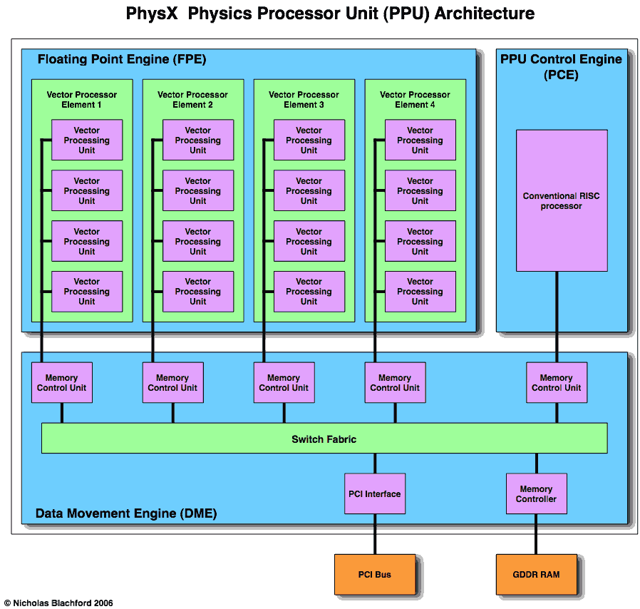
The Data Movement Engine (DME)
The PPU has a potentially vast amount of floating point power available, this however is of no use unless all the floating point units can be kept fed with data, the Data Movement Engine is responsible for doing this.
The DME is comprised of 5 memory control units, an external memory controller, a PCI bus interface and a “switch fabric”.
The switch fabric is a network of switches and busses which allow all the different units to talk to one another. In this case the switch fabric has 7 x 256 bit bidirectional ports, the number of units which can be talking simultaneously is not specified.
The work done in the Data Movement Engine is controlled by a series of 5 memory control units. 4 of these are connected to the Vector Processor Elements in the Floating Point Engine, the 5th is connected to the PPU Control Engine.
Each memory control unit contains a block of RAM and it moves data to and from it. This will mainly involve passing data to and from the external RAM and the vector processor element it is connected to, with the memory controller unit’s RAM acting as a buffer in between. They are not limited to this however and can also move data to and from the other memory controller units and the PCI bus.
You may wonder why it doesn’t just move data directly to or from the vector processors but this is done to make the usage of the external memory bus as efficient as possible. Moving data in big chunks is faster than moving data in small chunks so doing this will increase performance. Keeping data in on-chip buffers also allows data to be moved around the chip without going to main memory, again saving memory bandwidth.
The connections to the Switch Fabric and the Vector Processor Elements are separate so it looks like two types of communication can be operating simultaneously. For example, data could be written to one of the Vector Processing Elements while other data is being read in from external memory.
The Floating Point Engine (FPE)
The Floating Point Engine is the part of the PPU which does the real work, it performs all the actual physics calculations.
The FPE is made up of 4 Vector Processor Engines (VPE) and each of these is in turn made up of 4 Vector Processor Units, giving you in effect 16 vector processing cores.
The Vector Processing Units are not normal CPU cores but do contain some of the components normally found inside them along with some decidedly non-standard units.
All the data processing is done on 32 bit values stored in 16 floating point registers or 8 integer registers, there are likely other registers for program control and predication (a technique used in place of branches).
The execution unit appears to do vector processing with 6 elements whereas the normal is 4, this unit also contains a standard integer processing unit. It is not described in any detail in the patent but if it is anything like variant 1 the execution unit will use a hybrid processing model. This will issue a single integer instruction and a 6 part vector instruction as a single VLIW (Very Long Instruction Word) instruction.
The Vector Processor Units also contain a set of internal memories one of which is dedicated to storing the program being executed. There is also an “Inter-Element Memory” which is used to store data for processing. This is really a pair of memory blocks (A and B). At one point bank A is accessed by the processor while bank B can be accessed by the Memory Control Unit. When the processing and any data transfer is complete the access to these memories “switch” and the processor uses bank B while bank A is accessed by the memory control unit. This technique allows both memories to be accessed at full speed simultaneously, it is in effect a hardware double buffer.
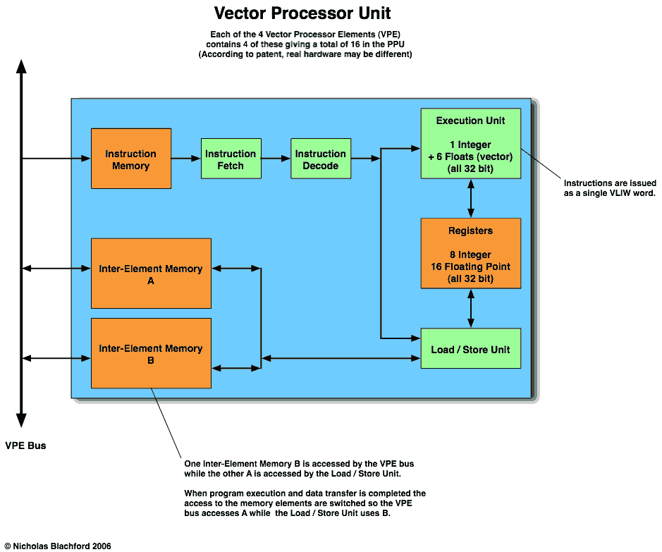
The amount of memory making up the internal memories is unknown but based on figures given in the description of variant 1 there should be at least 16 Kbytes per Inter Element Memory, giving a total of around 512 Kbytes memory in the Floating Point Engine.
If this arrangement is used in the final implementation the PPU should be capable of a theoretical 208 instructions per cycle (6 multiply-adds + 1 Integer) x 16 VPEs. This is nearly 3 times what the Cell processor in the PS3 can theoretically do and up to 50 times what any current conventional (single core) desktop processor can theoretically do. This equates to 96 GigaFLOPS for each 500MHz, the clock speed has not been announced but should be in the 500MHz - 1GHz range.
It should be noted that Ageia have not released any details on the actual silicon yet so we don’t at this point know if the full 16 VPEs are present in the final product, what the on-board memory sizes are and what clock speed the PPU runs at. The numbers indicated in the patent could, and probably have changed.
We do know some solid details though:
Manufactured by TSMC
125 Million transistors
182 sq. mm in 130nm
128MB GDDR3
28 watts (entire card)
Boards containing the chip are to be manufactured by ASUS and BFG.
--
Lets Get Physical: Inside The PhysX Physics Processor
Part 3 - The Alternative And Others
© Nicholas Blachford 2006